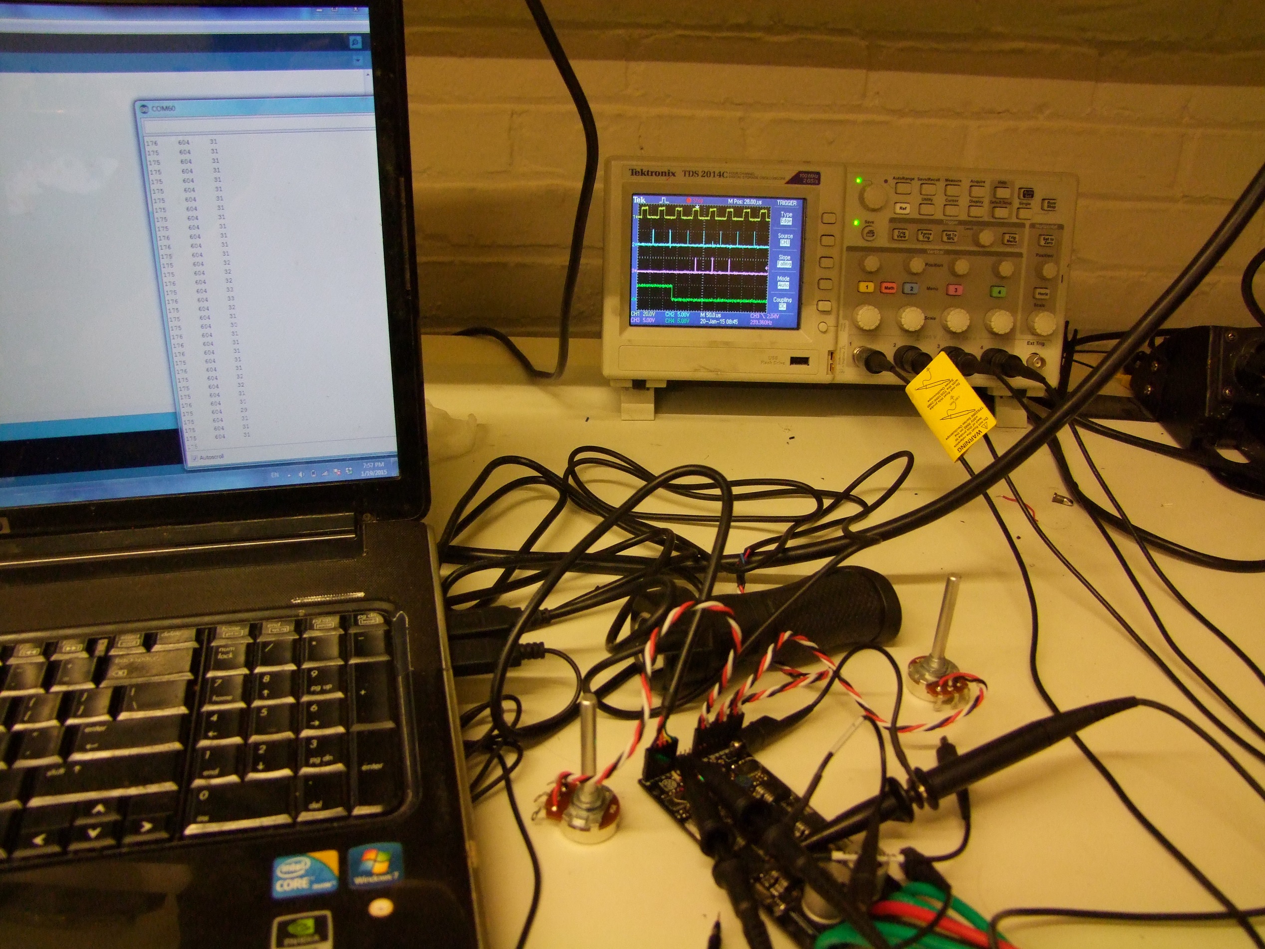
When I last talked about RageBridge, I was attempting to write current and throttle sampling code while on the plane to Shenzhen. I’m proud to say that every line of that session was scrapped because none of it made sense whatsoever. Do not attempt to code at 39,000 feet altitude after your complimentary in-flight red wine.
But as I promised, here’s the whole story of RageBridge v2 development up until now. The revision 1 boards came a week and a half before I left for China, so I was pretty much only able to put it together while tending to the end of semester project rush. The firmware was going to be sufficiently different that I couldn’t just plop the “production” RageBridge v1 firmware onto the chip, but some basic pin toggling showed me that all the hardware does work. In fact, the version 1 board claimed its first victim by slamming a poor RS-380 motor back and forth at full power 10 times a second…

Delicious version 1 boards arrive from Myro. These are 2oz copper boards – I wanted 4oz, but Myro informed me that their 4oz design rules need 10/12 (trace width / minimum spacing).
Maybe I’ll take the effort to try and route it with 12 mil spacing, which would be an immense undertaking and I might as well start from scratch… anyone have any (preferably inexpensive) PCB house recommendations that can do 10/10 in 4oz?

The same day, I commandeered the EE lab from the How to Make (a mess out of) Almost Anything students to assemble the board. I had, at this point, a few doubts about the sheer density of SMT component placement, such as small passives next to the larger inductor and capacitors in the logic power supply. These were echoed a bit by SeeedStudio when I showed them the board, but it is resolvable with a few minor design tweaks.

This firmware hacking session brought to you by Bawls Guarana. I wish you could find this stuff more readily, but if that were the case, I would have probably already died.
Before I started toggling pins, I first had to make a new Hobbyking Programming Socket Thing. I had one that I may have lent out to someone, but forgot who it could have been, so I considered it lost. This happens to something like 1/3rd of my stuff – lend it to a wide-eyed froshling, then immediately forget who it was. Some times, it even makes it back to me and I no longer remember the person and why I am being given something of mine that I swear was buried deep under a mountain of parts.
One bug I ran into right away: The gate drives wouldn’t enable. A little bit of prodding with an oscilloscope led me to discover that they were not receiving a power supply. Weird, but the 5v logic rail is feeding into the chip fine, and the chip is enabled, so the charge pump should be running…
That was when I discovered that I had mislabeled the charge pump pins when transcribing from datasheet to Eagle part.

On the A3941, there are a lot of doubled pins, like CP1/CP2, VBB, GND, and the like. In my infinite wisdom, I thought that VREG needed its own capacitor like CP1/CP2 does, instead of just needing to be 2 pins connected together, and a capacitor goes between VREG and GND.
So that’s why the gate drive rail was not energized – no capacitor, no fun.
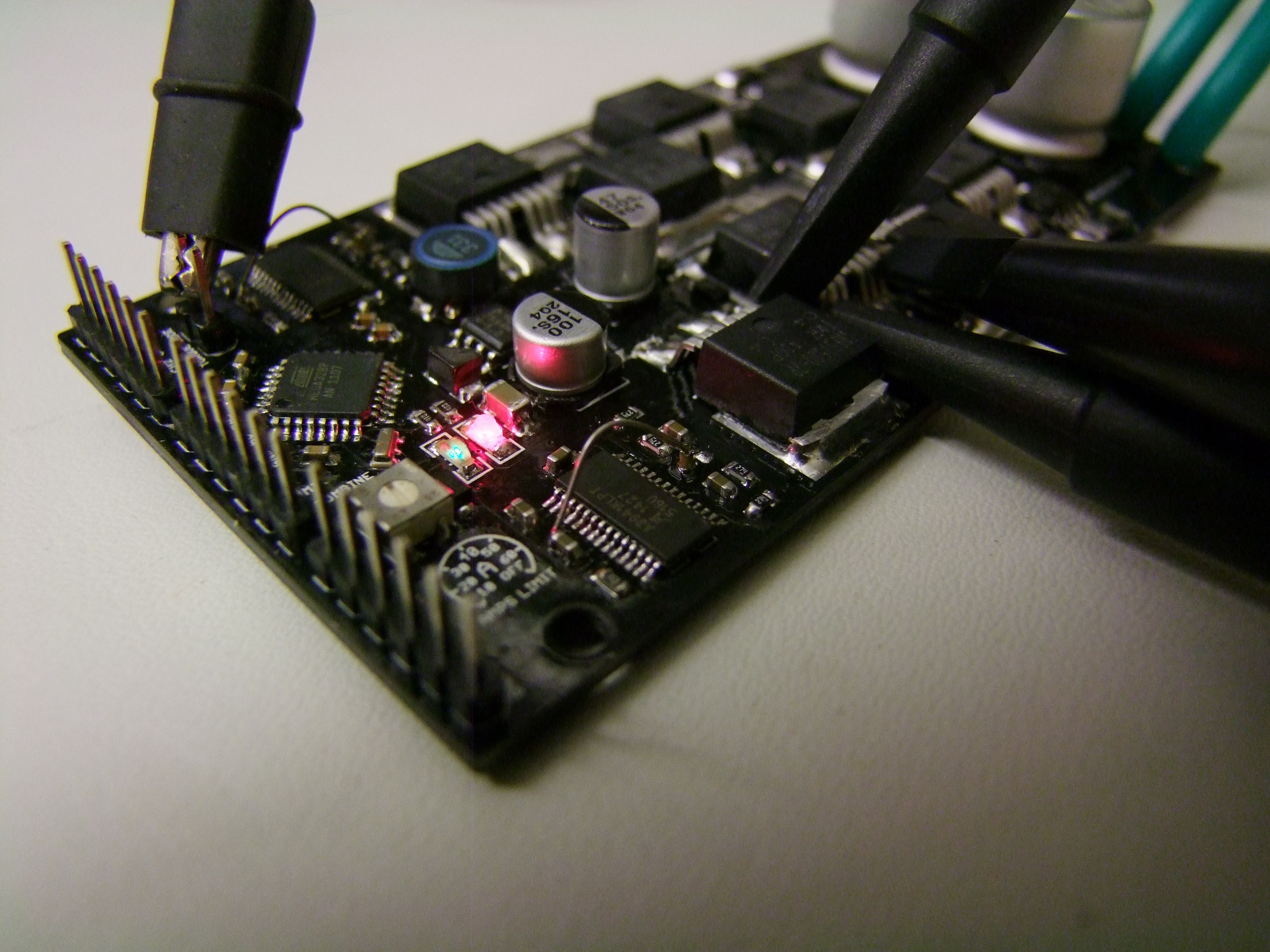
Oops. Pretty much all version 1 boards need some little wire jumps. I upturned the capacitor and soldered a jumper wire to the nearest available GND pin. It will do for firmware work!
Onto the firmware itself. For this version of Rage, I wanted to try having the ADC running synchronously with PWM, to capture a real-time current every time the controller switches. Not only does this simply offer vastly increased current control resolution for the DC controller, but synchronous sampling of current is basically required for torque control of brushless motors. There are some hackish ways around it, of course, like the Chinese e-bike controllers’ hardware-implemented cycle by cycle current limiting, but if your microcontroller has the ADC horsepower, it’s possible to implement many different closed loop control methods in software. And I looooove software.
The ATMega328’s wimpy ADC is just fast enough to do this, somewhat overclocked, at 15.6kHz PWM. It will up the temporal resolution of the Hysterical Current Limiter by more than 8x – currently, it runs 1000 times a second using whatever current reading it had last. However, because there is only 1 ADC on the chip, it has to be multiplexed to read the two current sensors on alternating PWM cycles. Therefore, the real sampling rate of the current is more like 8kHz – hence the 8x instead of 15x speedup.
Whatever the case is, I consider it more software practice than anything for Brushless Rage.
So here’s all the setup that had to happen, written in the form of a code novel:
  //Set up Timer 1 for the following:
  //Change the WGM bits on TCCR1A and B to Phase Correct 9 bit PWM
  TCCR1A &= ~(1 << WGM10);
  TCCR1A |= (1 << WGM11);
  TCCR1B &= ~(1 << WGM12);
  TCCR1B &= ~(1 << WGM13);
  //Change CS1:0 bits to no prescaling (31372hz pwm if we used 8-bit PWM that is standard, 15655hz with an extra bit of resolution)
  //As a result of the change to 9-bit, AnalogWrite( ) will take 0-511 instead of 0-255
  TCCR1B |= (1 << CS10);
  TCCR1B &= ~(1 << CS11);
  TCCR1B &= ~(1 << CS12);
  // Enable the Timer 1 overflow interrupt which will trigger a subroutine at the Bottom of every PWM cycle (16khz)
  TIMSK1 |= (1 << TOIE1); //Set TOIE1 and nothing else

  //Set up the ADC for the following:
  // Set ADC prescaler to generate a 1 MHz ADC clock; this increases the sampling speed 8x at a cost of ~ 1 LSB of resolution.
  ADCSRA = ADCSRA & 0b11111000 | 0x04; //Set ADSDP2, clear ADSP1:0
  // Set ADC to auto-trigger on Timer 1 overflow interrupt
  ADCSRA = ADCSRA | (1 << ADIE); //Set ADC conversion complete interrupt
  ADCSRA = ADCSRA | (1 << ADATE); //Set ADC auto trigger enable
  ADCSRB = ADCSRB & 0b11111000 | 0x06; //Set ADTS2 and ADTS1; clear ADCTS0, to select Timer 1 overflow as the trigger source
The way I code is to write more comments than there are lines of functioning code, in excruciating depth of exposition. I do this not only because I can’t be buggered to remember what these registers do in a week, but so other people who are forging into non-Arduino territory can more easily get what’s going on. Manual register configuration, sadly, is still how much of embedded programming works.
(I promise to rip on manual register configuration EVERY TIME I make a software post. Every. Time.)
Down at the bottom of this short testing code, I have the ISRs for the ADC and the PWM timer:
ISR(TIMER1_OVF_vect) {
  //Quick Pin D5 (Port D pin 5, "COMBINE" on the RB2 board) toggle to indicate we are in the ISR, for debugging
  PORTD &= ~(1 << 5);
  PORTD |= (1 << 5);

  slow_loop_prescale_counter++;
}

ISR(ADC_vect) {
  //Quick Pin D4 (Port D pin 4, "MIX" on the RB2 board) toggle to indicate we are in the ISR, for debugging
  PORTD |= (1 << 4);
  PORTD &= ~(1 << 4);

  byte low, high;
  low = ADCL;
  high = ADCH;
  hot_amps = (high << 8) | low;

}
The result of this is the following beautiful scope photograph:

The first trace up top is the PWM timer (Timer 1) overflow interrupt. This is the center of a PWM cycle, and is when the ADC is set off. A few (dozen) microseconds later, the ADC conversion complete interrupt service routine executes, which is the blue trace. At this point, a new current reading is available.
The purple trace is the ‘slow loop’, which runs a few hundred times a second using a software prescaler value. This is where inputs would be taken and new outputs calculated.

So how’s about the gate drives? Here’s a low-side trace directly at the gate of the FET. The total switching time is right around 1 microsecond… which is dismal for what I’m used to, but serviceable. Small fully-integrated driver chips are going to be wimpier than the IRS21844s that RageBridge v1 used, which are more often used on higher voltage systems with much larger devices.
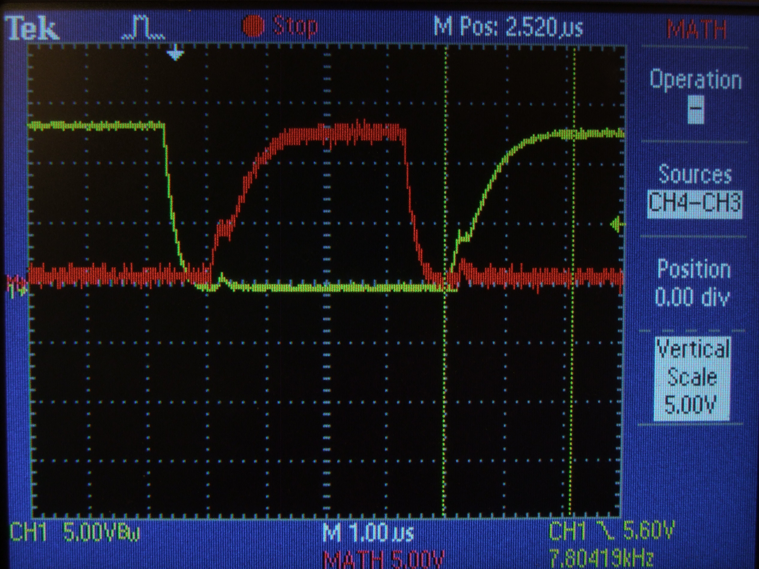
Some differential scope probing and a high-side gate waveform also appears. Unless you have a scope with completely isolated channels, don’t try to probe both the high and low side gates at the same time. This kills the gate.
What happens is, non-isolated scope probe grounds basically short the high-side gate drive through the ground clips, resulting in (usually) the gate driver dying. Don’t make my past mistakes, kids. You’ve been (repeatedly) warned.
This was the extent of the firmware work before I left for China. I tried telling myself I’d work on it while traveling, but hah, yeah right. Looking ahead, however, I made some design changes while in Beijing, and right before leaving Japan, I fired them off. Here is board revision 2, featuring…. well, not much difference. Some component placements have been relieved, but otherwise the power side circuitry is identical.

The biggest “duh” moment of handling my revision 1 boards was… there are through-hole headers everywhere. If I’m going to make a plate-style heat spreader like RageBridge v1, the through-hole header elements should be as closely grouped as possible to minimize holes and cutouts. In board revision 2, I tried shoving as many of the headers to the left as possible – fortunately, with a little trickery, I got all of them.
The “Fan” pins are still located inboard because there’s no other good place for them. The difference between the 5V supplied by this set of pins vs. what comes out of the 5V pins on the left, and the one that goes to the microcontroller, is that Fan power is taken from the ‘dirty side’ of the regulator, before the feedback pin and the 2nd output filter. That means it’s really dirty, chunky 5V, pretty much only good for running dumb loads like fans or gaudy lighting.
A week and some later, Revision 2 board arrives, along with…

… Brushless Rage!
Much to many peoples’ disappointment, Brushless Rage is going to be addressed when Brushed Rage is working and out the door, because it has a more critical ship date.
The backside of these boards is mostly made of soldermask-stop due to the high currents they’ll be conducting. Between this and the heat spreader plate will be a silicone thermal sheet layer to discourage shorting.
I actually have not assembled the version 2 board yet, because power circuitry-wise, version 1 and version 2 are identical – only the jumper and header row is different (…and the mis-routed pins have been routed correctly…) Since I have a functioning version 1 board already, it will be the focus for firmware development, and probably the first one to get blown up.
Since confirming that the ADC auto-trigger-upon-PWM-timer-interrupt system works, I next had to work out how to differentiate one reading from another. Here’s the issue, though: it would be easy to say “every other reading is either one or the other current sensor”. It’s not as easy to incorporate reading other analog inputs. I’m planning on building “analog mode”, for small silly rideable things, from the outset this time instead of promising to get around to it eventually.
While it would be “easy” to have an Arduino analogRead() plow through my already set-up ADC triggers every once in a while, in the interest of more robust code structure I decided to create a convoluted state machine to have the ADC interrupt routine determine what in the name of Sam it just read.
The basic idea is this. Every “slow loop” will request a new set of inputs (if in analog mode). The ADC ISR will merge these requests in with the current sensor reads automatically and update temporary holding variables just like it would for current. If inputs are being requested at the time the ADC is reading a current, then it will immediately reload the ADC, switch it over to the input under scrutiny, and read again, ideally finishing in time for the next current sample.
The full state logic I wrote down literally read like a bad text-based RPG.
You wake up in a dark room. You are an ADC. In your hand is a conversion result.You must figure out what variable to assign this conversion result to.> lookOn the wall besides you are three lists of the same words over and over, all scratched outexcept the bottom-most, and all stating that something is TRUE or FALSE.> read The list says:READING_CURRENT = FALSE;READING_CURRENT = TRUE;...andINPUTS_REQUESTED = FALSE;INPUTS_REQUESTED = TRUE;...andWHICH_CURRENT_TO_READ = FALSE;WHICH_CURRENT_TO_READ = TRUE;...It is clear the lists were made in your handwriting.You can read the last thing you write using (current), (which), or (inputs).When you are ready to guess what variable to assign your conversion result to, you can use (assign).> inputsINPUTS_REQUESTED is false.> currentREADING_CURRENT is true.> whichWHICH_CURRENT_TO_READ is true> assignTo take a guess at which variable to assign your conversion result to,type the name of the variable (ia, ib, inputs[0], inputs[1], or inputs [2])> ibBefore the memory bus was selected for a write, you were eaten by a grue.
See? It’s that simple!
The variable names are all real, and here’s how they interact.
Each PWM timer overflow interrupt, the READING_CURRENT flag is set, and the interrupt handler immediately sets the ADC going. When the ADC finishes about 15 microseconds later, the ADC conversion complete interrupt handler executes and sees that READING_CURRENT is true.
There are only 2 current sensors, so a simple logic inversion flag WHICH_CURRENT determines if it’s motor channel 1 or channel 2. It will save the current reading in the appropriate variable, invert the logic flag, set READING_CURRENT to false (since we’re done), and then move onto switching the ADC multiplexer to the other current sensor pin.
Every once in a while, the slow loop will call for an INPUTS_REQUESTED = true condition. When the ADC wakes up from converting, there’s two possible things that happen:
- That READING_CURRENT is true and that INPUTS_REQUESTED = true, which means the next cycle is an input read and has to start immediately, or
- That READING_CURRENT is false and that INPUTS_REQUESTED = true; which means the next cycle has to be a current read since THIS one was an input read, or
If this cycle was an input read based on the two state variables, then assign the reading to an input variable – this is in the form of an array, inputs[0:2] so it’s easy to iterate through.
Finally, based on the condition of the two state variables, the ADC interrupt handler will reassign the multiplexer to reflect the next desired read. If it’s an input, it will start the reading immediately. If no more inputs should be read, it sets INPUTS_REQUESTED = false so that part of the logic doesn’t happen until the slow loop causes it again.
It looks like this on a scope:
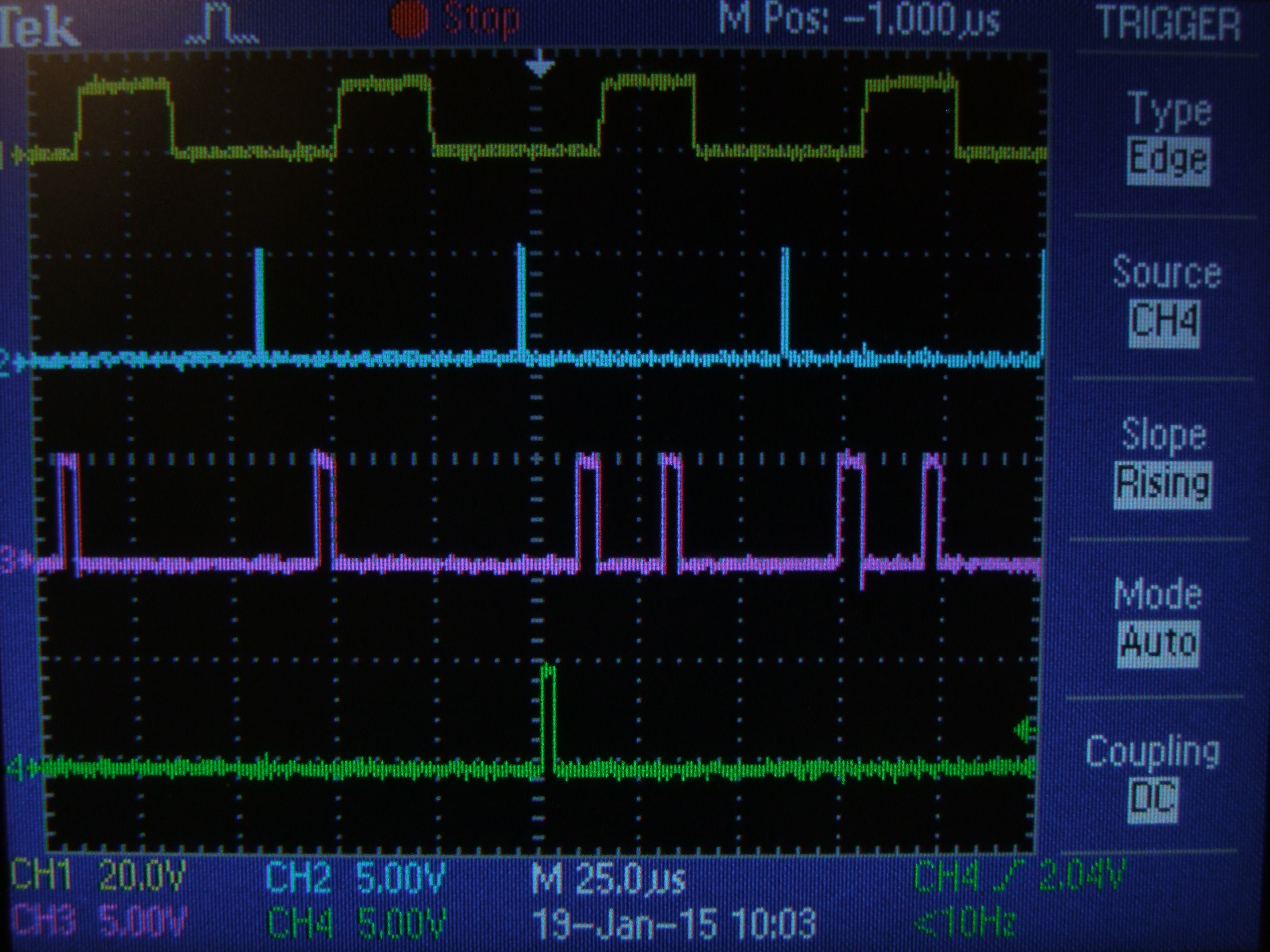
In this scope shot, channel 1 (yellow) is reading an output PWM that I hardcoded for convenience.
The next one down is the Timer 1 overflow interrupt handler, which sets off the ADC every PWM cycle.
The channel 3 (purple) spike that lags each channel 2 spike by about 15 microseconds is the ADC interrupt handler executing and reading current.
The channel 3 spike that immediately follows the rightmost two current reads are input reads. The first is inputs[0], the next inputs[1], and so on.
Channel 4 is the “slow loop” which, in this test code, serves only to set INPUTS_REQUESTED = true in order to irritate the ADC.
I was having trouble getting functional readings out of this setup, however. It seems like the current sensors were reading just fine, but the test inputs (which were potentiometers) were exceptionally noisy and inconsistent. I pondered for a while over this, and even refactored the above code from scratch to try and distill away any logic errors on my part.
No change. I even tried slowing down the ADC to only 4x the default Arduino speed – perhaps my potentiometers were too high impedance and it couldn’t fill the sample-and-hold capacitor fast enough? Seemed unlikely, but worth a try.

As the above scope photo shows, when I slowed the ADC down, the readings started running into each other and some of the input reads did not complete at all, being paved over by the externally triggered current reads.
I became suspicious when I noticed that the input reads succeeded when I grabbed the potentiometers in the right away. Uh oh…
To differentially diagnose, I put on some rubber gloves and tried again, figuring that my body impedance was messing with the potentiometers. Same result.
In disbelief, I grabbed a potentiometer that I knew to be working from using it to test other motor controllers, as well as a Hall Effect twist throttle from one of the scooters. Worked perfectly.
In summary, it is absolutely possible to have all three potentiometers you harvested from the depths of the shop to be scratchy or oxidized and making poor contact, and have that make you think it’s entirely your fault that you can’t write software.
Five minutes later, three perfect analog readings with three perfect in-sequence reads interleaved with current sensor reads. In this scope shot, the purple trace is only the portion of the logic that handles writing the inputs variable. It executes three times for three analog inputs.
Gee, that was a hilarious, rage-filled evening.
At this point, I’m ready to dive into writing the part of the firmware I actually care about – taking those inputs and doing something with them. I’m going to put in analog and R/C driving right away. Here’s the anticipated ‘state table’ of operating modes:
- R/C: Responding to signals in the 1100us – 1900us range, since it seems like that’s what radios put out by default. Failsafing behavior will check for valid/present pulse lengths on Channels 1 and 2, and shut down motor output if the signal is invalid.
In normal mode, channel 1 controls motor A, channel 2 controls motor B.
In MIX mode, channel 1 affects differential speed of the motors and channel 2 affects offset – what is usually called “Elevon” mixing, the most common configuration for robots.
In COMBINE mode, by popular demand, motor A and motor B PWM % is synchronized in the timer to turn rage into a 90-180A single channel controller.
MIX and COMBINE both selected is not a valid mode and will default to MIX.
In default and MIX modes, INVERT causes motor direction and speed to be swapped between A and B - ANALOG: By default, channels 1 and 2 respond to signals from 0.1 to 4.9 volts with ‘zero’ being 2.5 volts. Voltages below 2.5 cause that motor channel to run in reverse, above in forward (for your definitions of forward and reverse). The signal bounds are for fail-safe behavior since if control signals get disconnected, it is more common for them to hit the voltage rails (0 and 5v) instead of hover somewhere in the middle.
Channel 3 has no function. I mean, it COULD be an Invert input, but are you really going to drive your motorized couch upside-down?
Failsafe behavior requires signals be at 2.5v (within the deadband) at startup, or else the signals must be brought to 2.5v first, to prevent unintended couch acceleration.
In MIX mode, it assumes the use of a centered joystick or similar control setup, and its output behavior is similar to MIX mode in R/C.
In COMBINE mode, Rage becomes a 1 channel DC electric vehicle controller. The controller will respond to voltages of 1.0 to 4.0 volts, since that is the most common range for hand and pedal Hall Effect active throttles and potentiometer throttles set up as voltage instead of ohms (increasingly uncommon).
Motor outputs A and B are paralleled by default.
Channel 1 controls positive (driving) current from 0 amps to 2* IMAX amps.
Channel 2 controls negative (regen braking) current from 0 amps to 2 * -IMAX amps. Continually holding brake will not result in reversing. This is a bit of an unusual setup, but in my past experience, more people want their vehicle to coast by default instead of brake (drag braking) by default.
Channel 3 becomes a reverse switch depending on its digital logic state. - And of course, TTL Serial input, which is not high priority right now but will let Rage bust into the comically large servomechanism market. I suspect I will structure this as “simple serial”, compatible with many other small robot controllers – sending byte values 1 through 127 with 63 as center (0x01 to 0x7F with 0x3F center) controls channel 1 in forward and reverse, and 128 to 255 with 192 as center (0x80 to 0xFF with 0xC0 center) respectively for channel 2.
Sending 0x00 shuts down all motors to coasting condition.
In this case, Channel 3 is used as a ‘device select’ line.
These expectations might change once I get started coding. In particular, with respect to the ADC readings, I have yet to try to take any samples under power. It could be that system noise from the motors and FETs switching might make individual samples worthless. That might imply some more state machine trickery, such as if I have to read currents and inputs more than once, etc.
Right now, it’s anticipated that Rage will try to find the input mode on its own when it wakes up. After waiting for half a second upon power-up, it will…
- Obtain MIX or COMBINE status by reading those pins
- Check for bytes in the serial buffer; if there are, become Serial mode.
- Check for analog voltages at the 3 channel inputs, whether 1.0v or 2.5v depending on MIX/COMBINE mode; if there is the proper voltage present, enter Analog mode.
- Barring that, sit quietly for a few more milliseconds to listen for R/C pulsewidths; if there are valid ones, enter R/C mode
- If all of those steps fail, blink in futility, and re-attempt these steps once per second.
Man, it seems like “make it drive motors” is the easy part.